
Laboratory of laser microtechnology has long term experience with PLD. The main interest of involved scientific and application projects is focused on nanotechnology applications in deposition of oxide films (ZnO, TiO2, MgO) and metallic contact layers (Au, Pt, Cu, Ni, …). Currently, there are two deposition chambers installed in Laboratory which share two different ablating lasers. Their main parameters are briefly described below.
Deposition chamber УЛН – 5: Deposition of pure metals in form of contact (Ohmic or Schottky) layers is the main using of this chamber. Moreover, it is equipped by a particle separator for elimination of droplets for prevention of film contamination by particle ejected from target. Vacuum level reaches around 5×10⁻⁴ Pa and deposition process can be carried in vacuum only (and not in active atmosphere). A substrate holder (one single sample of maximum dimensions 15×15 mm) can heat the sample at maximum temperature of 700 °C during deposition process. A target holder works with two different targets, which can be changed during deposition.
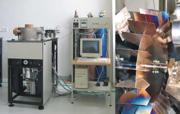
Fig. 1 Deposition chamber УЛН – 5 (right – particle separator)
Deposition chamber УЛН – 6: In contrast to previous chamber, it is not equipped by the particle separator, but on the other hand it permits depositions in active atmospheres up to 20 Pa (along with the vacuum depositions at around 5×10⁻⁴ Pa). Deposition of metal oxides is the main application of this deposition device. A special feature of this chamber is a wide span of substrate temperatures. The chamber is equipped by two different substrate holders: (1) – “classical” can heat substrate up to 600 °C and (2) – “cryogenic” permits deposition at the temperature of 77 K (boiling temperature of liquid nitrogen). A target holder is designed for two targets.
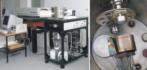
Fig. 2 Deposition chamber УЛН – 6 (right – inside arrangement of the substrate and target holders)
Solid state Nd:YAG laser Quanta Ray: (manufacturer Spectra Physics) emits at three different wavelengths (1064, 532, 355 nm). The pulse energy at the most used wavelength (355 nm) can reach maximally 400 mJ. The repetition frequency is 10 Hz without any possibility of adjusting of this parameter. The pulse-length (defined by FWHM) is approximately 10-15 ns.
Excimer (gas) laser COMPex Pro 205F: (manufacturer Coherent) works at wavelength of 248 nm. The pulse repetition frequency can be adjusted between 0.5 to 50 Hz and the maximum pulse energy up to 700 mJ. The pulse-length (defined by FWHM) is approximately 20 ns.
Pulsed laser deposition – examples of experimental results in ILC
Compact layers
Fig. 3 represents an example of compact layer deposited by PLD in ILC. The goal was deposition of thin (30 – 50 nm) MgO layer as isolating (dielectric and diffusion) barrier on GaAs and subsequently prepared functional layers on the surface of MgO. The finally optimised deposition technology consisted of the two steps deposition and final post-depositional annealing. The first step served for “seed layer” deposition (couple of nanometers thin layer deposited by ablation of MgO target). Second step was carried in O2 atmosphere (15 Pa) but the target was consisted of pure Mg. The substrate was heated at 450 °C. Finally, the film was annealed in pure O2 at atmospheric pressure for 10 minutes at the same temperature. Fig. 3 shows the result in SEM picture at the cross section.
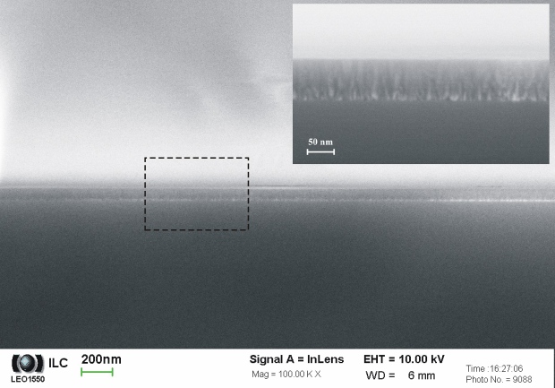
Fig. 3 MgO layer deposited at GaAs by PLD. Process parameters: 300 pulses MgO (450 °C, 1.10-3 Pa, laser 355 nm, 4,0 J.cm-2) + 6000 pulses Mg (450 °C, 15 Pa O2, laser 355 nm, 2,5 J.cm-2), annealing 10 minutes, 450 °C (O2 – atmospheric pressure).
Porous layers of high ratio „surface / volume“
This kind of layers are interesting for sensor applications where maximum active surface is inevitable. Equally, this parameter plays crucial role in catalytic applications, where certain crystallographic orientation and certain crystal surfaces with higher surface free energy are preferred. Titanium dioxide (TiO2) is an example of such compound. It crystallizes in three different polymorphs at room temperature and pressure (rutile, anatase and brookite) as well as in amorphous form. Pure (without rutile content) anatase porous structures were prepared by PLD. Firstly, amorphous TiO2 was prepared at cryogenically cooled substrates. Deposited structure grown at such metastable conditions exhibited high porosity (Fig. a). The porous nature of the deposited structure was partly preserved after annealing, however the structure crystallized to anatase phase. Fig. 4 compares appearance of TiO2 layer in amorphous state (Fig. 4a) and after annealing at 600 °C and subsequent phase transformation to anatase (Fig. 4b) [1].
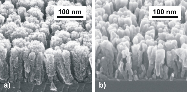
Fig. 4 TiO2 deposited on Si <100> by PLD. Process parameters: TiO2 target, substrate temperature 77 K, 9000 pulses, laser 355 nm, fluence 2.8 J.cm-2, O2, 5 Pa. a – as deposited state, b – state after annealing at 600 ° (60 minutes)
Modification of electrical parameters of semiconductor layers
An important number of PLD applications are semiconductor layers for electronic components. According to chemical composition of the targets and growth conditions there is possibility of “tuning” of their electrical properties in wide ranges. Chemical composition is the most important factor, however substantially different properties can be achieved by application of different process treatment at otherwise chemically the same films.
Fig. 5 compares influence of Al and Ga on electrical, optical and emission parameters of doped ZnO films prepared by PLD. Presented results were achieved by 4-points Van der Pauw Hall measurements, optical absorption spectroscopy and photo luminescence spectroscopy. Applied targets were doped in form of metal oxides (Al2O3 and Ga2O3) and three different concentration levels were used (0,15, 1 and 2 wt. %). The deposition conditions of all samples were the same (O2 atmosphere, 5 Pa, 400 °C, sapphire substrate). Ablating laser (KrF, 248 nm) worked at 10 Hz pulsing frequency, and 120 mJ pulse energy (fluency after focusing was around 2.8 J.cm-2). Closer details about experiments and results are presented in [2].
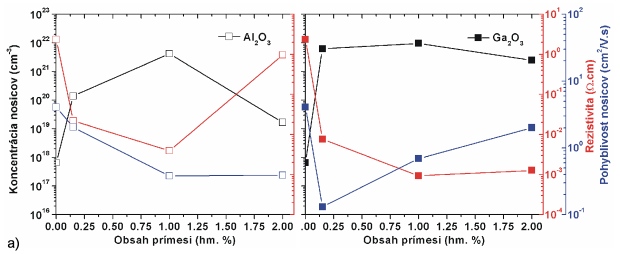
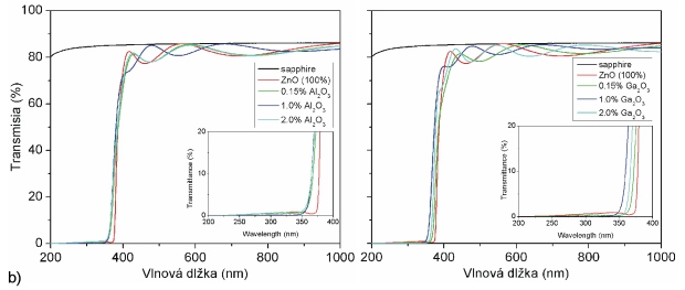
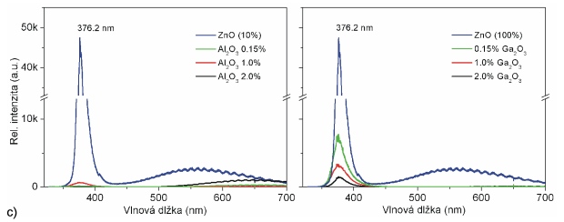
Fig. 5 Comparison of (a) electrical, (b) optical and (c) photo-luminescence of ZnO films doped by Al2O3 (left) and Ga2O3 (right) in dependence of doping concentrations.
Fig. 6 shows another example of ZnO films and modification of their electrical properties by process parameters during PLD. The film growth was carried in N2O atmosphere at different pressures 1, 5 and 10 Pa [3]. Different pressures resulted in different electrical resistivity, carrier concentration and Hall mobility, while intrinsic n-conductivity was preserved.
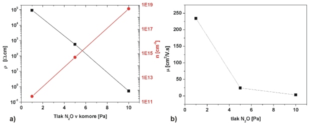
Fig. 6 Electrical properties of ZnO:N films (deposited on SiO2 substrates) in dependence of N2O pressure. Process parameters: ZnO target, substrate temperature 400 °C, 15 000 pulses, laser 355 nm, 2.8 J.cm-2, N2O, 1 – 15 Pa. a – film resistivity and carrier concentration, b – Hall mobility)
Deposition of layers on nanostructured surfaces by PLD
As an example of such PLD application can serve covering of GaP nanowires by ZnO. The aim of this task was create continuous ZnO layer with thickness of around 50 nm on GaP nanowires sidewalls and p-n junction at GaP/ZnO interface. Fig. 7 shows a pair of pictures, where the left one represents a low magnification view on covered nanowires and the right one captures the middle part of the nanowire with magnified detail.
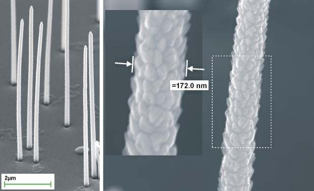
Fig. 7 GaP nanowires with ZnO layer. Left – covered nanowires and substrate, right – a middle part of the typical nanowire with a detail of a depicted part. Deposition parameters: ZnO:Al2O3 (1%) target, laser Quanta Ray (355 nm), fluence 2.8 J.cm-2, 4,500 pulses, 400 °C, 5 Pa (O2).
Pulsed Laser Deposition of ZnO nanowires
Nanowires represents very interesting nanostructures and attract huge scientific interest nowadays and they are considered as perspective “building block” elements in nanotechnology. In principle, there are two main groups of techniques suitable for their growth: (1) In the first case, it involves the direct growth (crystallization) of the vapours on the nucleus and then on the growing interface of the nanowire. This growth mode is called the “Vapour – Solid” (VS). (2) The second group can be called as an assisted (catalytically supported) growth, which is localized and proceed at the interface between a droplet of saturated solution of the metal catalyst (typically Au, Cu, Pt) and the nanowire material (this method is commonly referred to as that “Vapour – Liquid – Solid” – VLS).
PLD is considered as a proper method for nanowires growth and referred results has widely been confirming these perspectives. Fig. 8 represents an example of ZnO nanowires prepared in ILC by application of VLS method with copper particles as catalyst material.
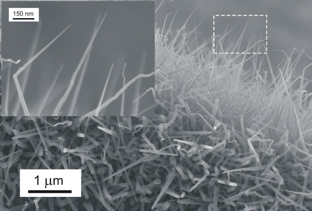
Fig. 8 ZnO nanowires prepared at Si <111> by PLD. Process parameters: ZnO target, substrate temperature 600 °C, 9000 pulses, laser 355 nm, 2.8 J.cm-2,atmosphere: Argon 10 Pa.
References
[1] Bruncko, J., Vincze, A., Netrvalová, M., Šutta, P., Michalka, M., Uherek, F.: Cryogenic pulsed laser deposition of ZnO, Vacuum 86 (6) (2012), pp. 684-688. (http://www.sciencedirect.com/science/article/pii/S0042207X13000377)
[2] Bruncko, J., Šutta, P., Netrvalová, M., Michalka, M., Vincze, A., Kovac, J.: Comparative study of ZnO thin film prepared by pulsed laser deposition – Comparison of influence of different ablative lasers, Vacuum (2016), http://dx.doi.org/10.1016/j.vacuum.2016.09.013. (article in press) (http://www.sciencedirect.com/science/article/pii/S0042207X16305644)
[3] Bruncko, J., Vincze, A., Netrvalova, M., Uherek, F., Sutta P.: Pulsed laser deposition of ZnO in N2O atmosphere, Applied Physics A, (2010) 101: 665-669. (http://link.springer.com/article/10.1007/s00339-010-5949-9)

|
|
|
|